Graphene: Weak spots turn to be strengths that can be exploited in electronics

Grain boundaries in layers of graphene sheets enhance the strength of the material, instead of being weak spots as believed so far.
A Rice University study goes to prove that perfection may not always be the best objective to seek.
The winding thread of odd rings of five and seven atoms at the border of two sheets of graphene, create a "sizable electronic transport gap," or band gap required in semiconductors.
This could prove valuable to manufacturers, according to Rice University scientists, who determined that at certain angles, these "sinuous" boundaries relieve stress that would otherwise weaken the sheet.
Growing polycrystalline graphene with precise misalignment of components will be a tough job but can be achieved using substrate with prescribed grain orientations that influence carbon groupings, says the team.
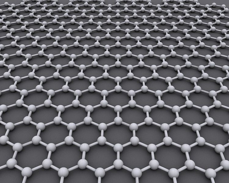
Graphene, the single layer sheet of carbon, does not grow as a perfect lattice of six-atom rings. The chemical vapour deposition confers "domains," or separately grown sheets that meet at these points.
Where they meet, irregular rows of five- and seven-atom rings adjust the alignment of the regular rows of atoms by compensating suitably for the angular disparity.
"If stress along the boundary were alleviated, the strength of the graphene would be enhanced," postdoctoral researcher Zhuhua Zhang who led the study said. "But this only applies to sinuous grain boundaries as compared with straight boundaries."
Theoretical physicist at Rice, Boris Yakobson and his team calculated the mechanical strength of grain boundaries to determine where the boundaries are inclined to bind and where they are likely to break under tensile stress.
Grain boundaries minimised the interface energy between sheets by forming pairs of rings called dislocations, where an atom shifts from one six-member ring to its neighbour to form connected five- and seven-atom units.
The band gap properties were seen to extend to the entire polycrystalline sheet, especially when the patterns repeat along the boundary.
One of Zhang's simulations of energetically "preferred" grain boundaries was a near-perfect match for the asymmetric boundary cited in a 2011 paper in Nature that said grain boundaries severely weaken the mechanical strength of graphene membranes but do not as drastically alter their electrical properties.
The study is published in Advanced Functional Materials.
Graphene in LED
Meanwhile, in further applications of graphene in electronics, University of Manchester and University of Sheffield researchers created an LED using atom-thickness of two dimensional crystals.
This paves the way for flexible, transparent and ultra-thin light emitting devices for mobile phones, tablets and televisions from 2D 'designer materials'.
Freddie Withers, Royal Academy of Engineering Research Fellow at The University of Manchester, who led the production of the devices, said: "As our new type of LED's only consist of a few atomic layers of 2D materials they are flexible and transparent. We envisage a new generation of optoelectronic devices to stem from this work, from simple transparent lighting and lasers and to more complex applications."
© Copyright IBTimes 2025. All rights reserved.


